
 PCB Design & Layout Services

Expert Printed Circuit Board Design for Demanding Applications
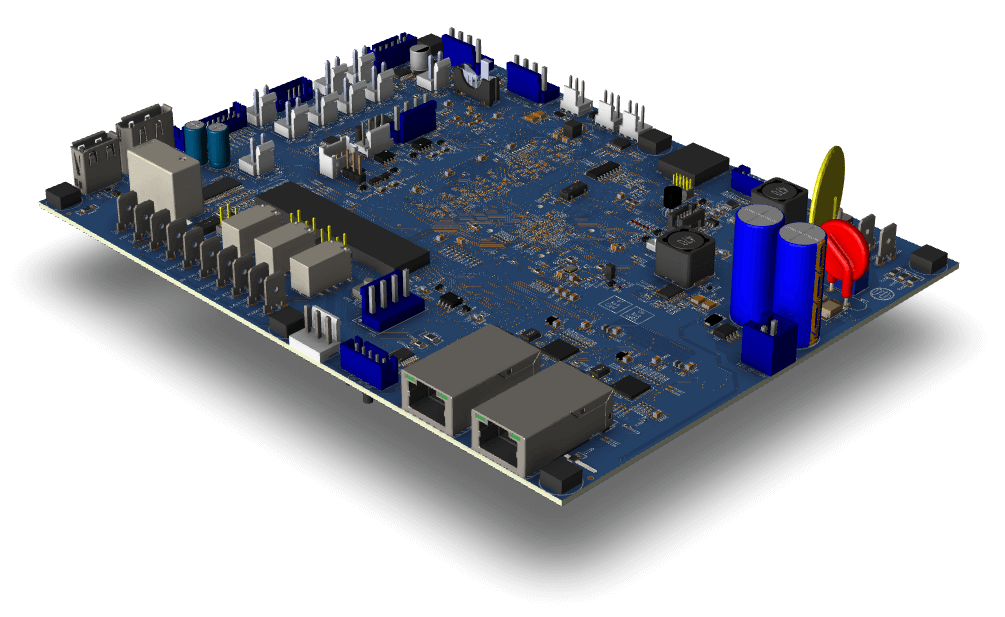
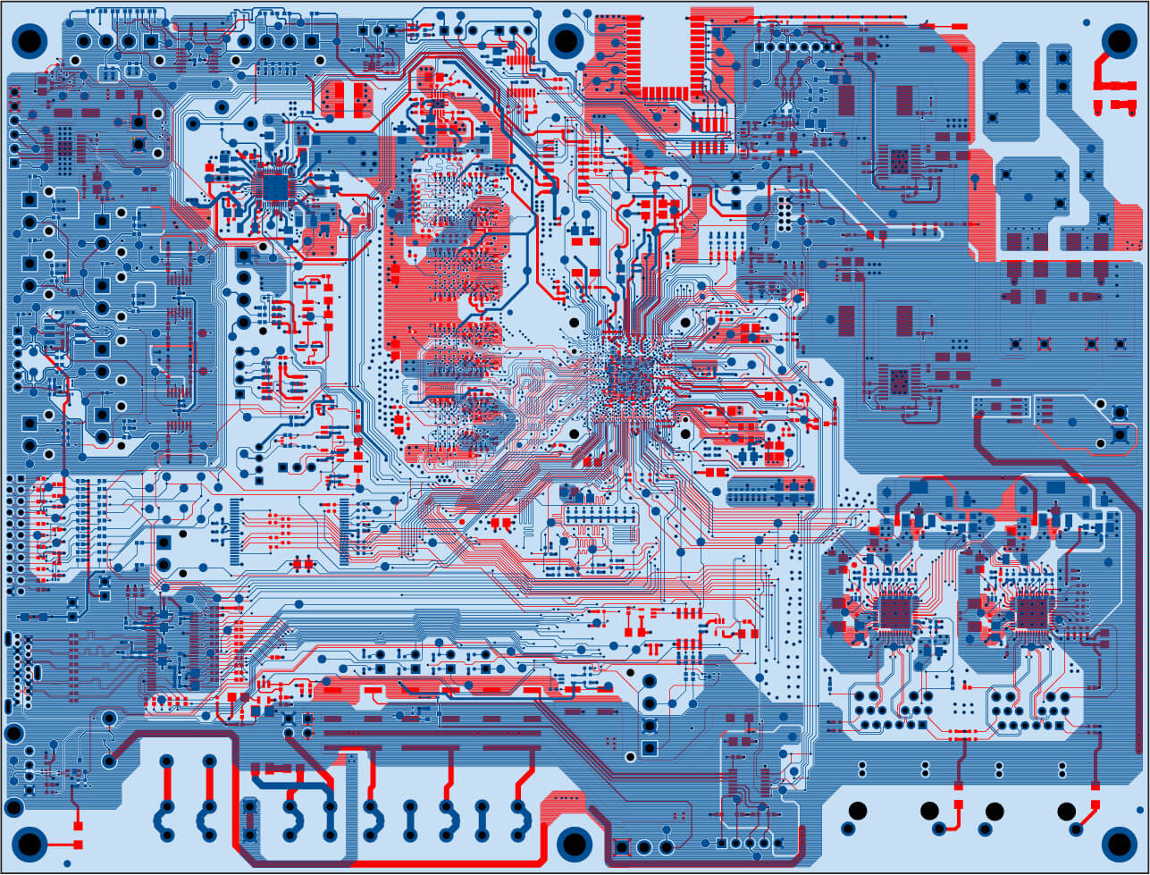
We have been doing advanced Printed Circuit Board (PCB) design since 2002 – That vast experience at the initial PCB layout and hardware design stage can reduce industry compliance testing issues later on. Custom PCB layout, schematic entry, and hardware architecture design are our core competencies at DE Design Works, whether for rugged industrial environments, medical embedded products, or reliable military applications to keep our service members safe – our experience saves your project time and NRE.
- Circuit Design & PCB Schematic
- Custom PCB Design & Layout
- Costed BOM
- Mechanical Design / ID / GUI
- System Design / Systems Integration Design
- Supply Chain & Obsolescence
PCB & PCBA Expertise
- Analog Systems and Sensors
- High Speed Digital and Networking
- Wireless Connectivity such as BLE, Wi-Fi, and LoRa
- EMC / EMI or RFI
- Low Power and Battery Operated
- Industrial Controls and IoT
- Power Systems
- Motor Control
- Radio Frequency (RF)
- UI/UX, and Touch Screens
- User Interface & Overlay Design
- Mechanical Design
- Military
- Medical
- Commercial Products and Appliances
- Broad Market Industrial
Why Choose DE Design Works for PCB Hardware Design?
Integrated Engineering for Real-World Products
Modern electronic products require tightly coordinated hardware, firmware, and connectivity decisions. Misalignment across disciplines introduces risk, rework, and delays. DE Design Works brings these capabilities together, enabling system-level thinking from the start.
Senior Engineering Expertise Based in the US
Our engineers bring deep experience across industrial, medical, and military environments. We design with compliance, reliability, and long-term lifecycle considerations in mind, ensuring solutions perform beyond the prototype stage. Our entire team is based in the United States.
A Risk-Reduction Mindset
We focus on architecture, verification, and disciplined execution to identify and manage risk early. This approach helps teams avoid surprises later in development and supports confident decision-making throughout the project lifecycle.
Adaptive Partnership
DE works seamlessly with internal teams to fill gaps in specialized engineering technology. We support full product development, platform modernization, new technology integration, troubleshooting, and obsolescence management—tailored to each client’s needs and development stage.
Predictable Execution
Our proven processes emphasize clarity, accountability, and dependable outcomes. Clients rely on DE for steady execution that keeps complex electronic product development moving forward.
PCB Tools & Expertise: Read Why DE Design Uses Altium 365
At DE Design Works, we use Altium 365 because it's built for the high standards Blue Chip companies expect. These organizations can’t afford delays, redesigns, or IP vulnerabilities—and neither can we. That’s why we’ve built our workflows around the powerful Altium 365 cloud-native platform.
Frequently Asked Questions (FAQs)
Is DE experienced at complex PCB design such as high speed or high-power controls?
Yes, we have experience in SMT and through hole, BGA, high speed digital, and analog layout best practices for simple or multi-layer (8-layer PCB design, for example). If you are looking for specific PCB design experience, please fill out our form with your needs and we would be happy to reply.
What is the advantage of working with DE on a custom PCB design?
DE Design Works has a team of specialists who focus on PCB hardware and systems integration (and embedded firmware for our PCB solutions). Their committed R&D efforts result in shorter lead times, reduced non-recurring engineering costs, and stable, pre-tested hardware core circuit designs. DE Design Works has an extensive set of advanced technologies and industry partnerships that guarantee tailored solutions for intricate requirements, leading to quicker market entry and future-proof designs. We also use the latest PCB design tools like Altium 365 that allow seamless collaboration with our customer’s product development teams.
How long does a PCB design project take? How long does it take to design a PCB?
The duration of a PCB design project typically ranges from 2 to 3 months for schematic and layout, assuming a thorough initial assessment and no significant design changes. Simpler projects may be completed more quickly, while more complex designs can extend beyond this timeframe. Additionally, prototyping and testing generally require about a month. Precise timelines depend on the project's complexity, required features, and testing iterations. DE writes a clear statement of work proposal with detailed time estimates and costs associated with each step. And we are always willing to share how our PCB prototyping capabilities often help our customers cut weeks and months from their schedules.
How much does a custom PCB design project cost?
A custom PCB design project typically starts at $30,000 and can top $100k, depending on the complexity of the design and what the project goals are. This starting point likely covers schematic design, layout, mechanical considerations, design reviews, prototyping, then bring-up testing and BSP firmware. While many design services may quote much lower PCB prototype prices, we do not simply ship our customers untested Rev-A prototype boards and wish them good luck. We are happy to talk over your project and budget to see if DE is a good fit for your specific project goals.
Does DE work with startups?
Yes, DE Design Works does work with startups, but it depends on the specific project requirements and alignment with DE capabilities. Startups with well-defined product goals, realistic budgets, and a clear path to market are more likely to benefit from our expertise. DE is selective in choosing projects that leverage their advanced engineering capabilities and R&D resources, ensuring a successful and efficient collaboration.
How does DE align technology with my needs?
DE Design Works aligns technology with your needs through a thorough assessment of your project goals and requirements. By leveraging their expertise in embedded systems and PCB design, they select the best technologies to optimize performance, reduce risk, and accelerate time-to-market, ensuring a tailored solution that meets your objectives.
Our Process

When Engineering Custom PCB Design Is the Right Choice in Electronic Products
We've had a lot of conversations with potential new customers where the PCB decision gets treated like a procurement question.
Someone on the team identifies a module or development board that gets the system running. It works. It proves the concept. And then, six months later, that choice has quietly shaped the product architecture in ways nobody fully anticipated — limiting what can be changed, locking in vendor dependencies, or creating constraints that show up at exactly the wrong moment in a product program.
Custom PCB design isn't always the right answer. But the decision about whether to pursue it deserves more strategic weight than it usually gets.
Key Takeaways
- Custom PCB design is a strategic decision, not a technical preference — it should be evaluated through the lens of system control, lifecycle risk, and long-term ownership.
- Off-the-shelf and modular solutions are often the right starting point. The question is whether they remain the right answer as product requirements mature.
- The real cost of the wrong PCB strategy shows up late — in integration constraints, redesign cycles, and support complexity — not at the point of selection.
- Custom PCB decisions affect firmware architecture, component availability, manufacturing, and regulatory posture across the full product lifecycle.
- The right choice depends on where the product is going, not just where it is today.
The Question Project Leaders Should Actually Be Asking
Conversations like this, start with "what can we use to get this working?" That's a reasonable place to begin. The more important question — the one that belongs at the leadership level — is: "What does this decision cost us over the life of this product?"
Off-the-shelf modules and development platforms have real advantages. They compress early development timelines. They reduce upfront engineering investment. They let teams validate concepts without committing to a full hardware design. For early-stage exploration, that flexibility is genuinely valuable.
The problem is that those same decisions tend to accumulate constraints. Physical size and form factor are fixed. Interface options are limited to what the module was designed for. Component choices belong to someone else's roadmap — not yours. And in long-lifecycle products, that loss of control compounds over time.
The PCB decision isn't just about what works now. It's about what you're building toward.
Where Off-the-Shelf PCB Solutions Start Creating Risk
We’ve seen prospect customer teams that have gotten surprisingly far on development boards and commercial modules and hobbyist boards. Far enough that there's real organizational momentum behind the architecture by the time the limitations become visible.
That's when the conversation gets difficult.
The limitations usually surface in a few predictable places. Physical integration into the enclosure or end product is clunky and bulky making manufacturing laborious, expensive, and non-professional. Performance headroom is constrained in ways that weren't apparent in early testing. Interface and connectivity requirements evolve beyond what the platform was designed to support. Or a supplier changes their roadmap and suddenly a component that the whole system depends on is approaching end-of-life.
None of these are catastrophic on their own. But they tend to arrive together, late in development, when the cost of changing direction is highest.
Custom PCB Design as a System-Level Decision
The reason custom PCB design deserves leadership attention is that it's not really a hardware decision. It's a system-level decision with downstream consequences for firmware, manufacturing, compliance, and lifecycle support and total cost of final goods assembly.
A custom PCB gives the engineering team control over the full architecture — processor selection, memory configuration, power design, interface layout, thermal behavior, and connector choices. Those degrees of freedom aren't just nice to have. In products that need to remain field-serviceable for ten or fifteen years, they're often the difference between manageable evolution and expensive redesign.
That control also matters for firmware. When the hardware is purpose-built for the application, firmware architecture can be designed around it cleanly. When firmware has to work around a module's constraints and assumptions, complexity accumulates in ways that create maintenance burden over time.
The interdependence runs in both directions. A PCB decision is also a firmware decision. A firmware decision is also a lifecycle decision. Leadership teams that see these connections early make better choices than those who evaluate each domain separately including security and IoT remote over the air updates that should be core to the architecture design, not after thoughts.
What the Tradeoff Actually Looks Like
Custom PCB design requires more upfront investment. There's no way around that. Design time, layout, fabrication, bring-up, validation — these take longer and cost more at the front of the program than reaching for an existing module.
But that comparison is incomplete unless it accounts for what happens later.
Redesign cycles that stem from platform limitations are expensive — not just in engineering time, but in schedule impact across the whole program. Vendor dependencies that constrain component choices carry real lifecycle risk. Support complexity that builds on top of a constrained architecture has a cost that shows up every year the product is in the field.
In my experience, the teams that regret custom PCB decisions almost always regret moving to them too late, not too early. The teams that struggle with off-the-shelf decisions tend to reach the same conclusion at a point where changing course is more painful.
The tradeoff is real. But it's rarely as symmetric as it looks at the point of selection.
Timing the Decision Well
There's no universal rule for when custom PCB design becomes the right choice. But there are signals worth paying attention to.
When the product has moved past concept validation and into architecture definition, it's worth asking whether the platform it's running on can carry it forward. When integration requirements — physical, electrical, or mechanical — are becoming more specific, that's a signal. When firmware complexity is growing in ways that feel constrained by the underlying hardware, that's worth examining. When the product roadmap extends beyond five years, the lifecycle control that comes with a custom design starts carrying more weight. If your product cannot be updated in the field, it is not “smart” device, or there is not a roadmap for data analytics and IoT connectivity, and security- just functionality it is time to plan and define the use case and document requirements.
These aren't bright lines. But they're the kinds of questions that belong in the engineering leadership conversation, not just on the hardware team's checklist.
One Last Thought
The PCB decision is one of those choices that shapes the product long after it's been made. Not dramatically — it doesn't show up as a single failure point. It shapes what's possible, what's maintainable, and what redesign looks like when it eventually becomes necessary. It can solve your global supply chain concerns and lower your total costs at the same time.
That's why it belongs in the strategic conversation, not just the technical one.
The right answer depends on where the product is going, what the team needs to control, and how long the organization plans to own the outcome. When those factors are weighed honestly, the decision usually becomes clear — even when it's not easy.
If your team is working through a PCB architecture decision — whether to stay on an existing platform, migrate to custom hardware, or evaluate the tradeoffs for an upcoming design — we're happy to think through it with you. Reach out to the DE Design Works team.
Frequently Asked Questions
When does custom PCB design make more sense than an off-the-shelf module?
When the product has moved past concept validation and has specific physical, electrical, or interface requirements that a module, or PLC, can’t accommodate cleanly. The stronger signal is usually lifecycle: if the product needs to be supported and evolved over many years, the control that comes with custom hardware typically justifies the upfront investment.
What are the hidden risks of staying on a development board or commercial module too long?
The most common issues are loss of control over component availability, physical integration constraints that limit how the product can be packaged, and firmware complexity that builds up around the platform’s limitations rather than the application’s actual requirements. These rarely surface until late in development, when changing direction is costly.
How does the PCB decision affect firmware development?
Significantly. A custom PCB lets firmware be architected around the application’s actual requirements — memory layout, interface configuration, power states, timing behavior. When firmware has to work around a module’s fixed constraints, complexity accumulates over time and becomes a maintenance and evolution burden.
Does custom PCB design always cost more?
It requires more upfront investment — design, layout, fabrication, validation. But the full cost comparison has to include what off-the-shelf limitations cost later: redesign cycles, vendor dependencies, support complexity, and lifecycle risk. In long-lifecycle products, the math often looks different once those factors are included. In many cases a custom PCB is much more cost effective, ands depending on what and how many you are building it can be orders of magnitudes of savings and drastically reduce your supply chain risk at the same time. Quality custom PCB design takes professional engineering but it is an investment that pays off for years.
What questions should engineering leadership ask before making a PCB architecture decision?
The most useful ones are: Where is this product going over the next five to ten to fifteen years? What do we need to control to support and evolve it? What are the realistic risks of staying on the current platform? And what does redesign look like — and cost — if we defer this decision? Those questions shift the conversation from technical preference to strategic tradeoff, which is where it belongs -first.